


Categories


Latest Products
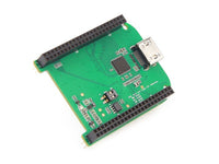


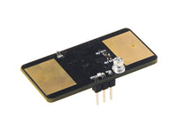
PCF8591 module/ AD/DA conversion module/ modulus to modulus conversion/ 4 PIN Dupont line included

- Order within
Shipping list:
1. PCF8591 module *1
2. 4 PIN female dupont line * 1
Data download address: http://pan.baidu.com/share/link?Shareid = 3844 & UK = 590225187
PCF8591 AD/DA chip introduction
PCF8591 is a monolithic integrated, single power supply, low power consumption, 8-bit CMOS data acquisition device. PCF8591 has four analog input, 1 analog output and 1 serial I2C bus interface. Three address pins of PCF8591, A0, A1 and A2 can be used for hardware address programming, allowing 8 PCF8591 devices on the same I2C bus without the need for additional hardware. Address input and output, control and data signals on the PCF8591 device are transfered through dual bidirectional I2C bus, in the form of serial transmission.
PCF8591 main performance index:
Single power supply
operating voltage range of PCF8591: 2.5V to 6V
Low standby current
input/output through I2C bus serial transmission
PCF8591 addressing through three hardware address pins
PCF8591 sampling rate is determined by the rate of I2C bus
4 analog input, can be programmed into single-end or differential input
Automatic incremental channel choosing
PCF8591 analog voltage range from VSS to VDD
PCF8591 built-in track and hold circuit
8-bit successive approximation A/D converter
DAC gain was achieved by 1-way analog output
Product description
1 module chip uses PCF8951
2 module supports external 4-way voltage input collection (voltage input range 0 to 5v)
3 module is integrated with photocell, can collect precise environmental light values through AD
4 module is integrated with thermal resistor, can collect precise environmental temperature values through AD
5 module is integrated with 1-way 0 to 5V voltage input collection (adjust input voltage by blue potentiometer)
6 module include power indicator light (light up when module is power on)
7 module include DA output indicator light, when the DA output voltage of the module interface reaches a certain value, the light will be lit up; the bigger the voltage, the lighter the light will be;
8 module PCB size: 3.6 cm * 2.3 cm
9 standard double-sided board, board thickness 1.6 mm, nice layout, through-hole around, hole diameter:3 mm, easy to fix
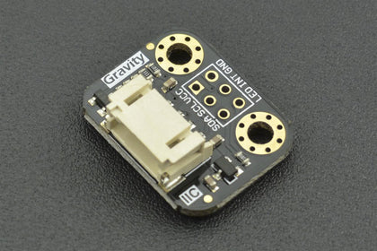
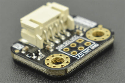
Module interface specification
On the left and right side of this module, there are 2 expansion raws of pin strip, detail as follows:
On the left: AOUT chip DA output interface
AIN0 chip analog input interface 0
Module red short-circuit cap instructions
There are three red short-circuit module cap, used separately as follows:
P4: connect P4 short-circuit cap, select thermistor to connect to the circuit
P5: connect P5 short-circuit cap, select photocell to connect to the circuit
P6: connect P6 short-circuit cap, select 0 to 5v adjustable voltage to connect to the circuit
AIN1: chip analog input interface 1
AIN2: chip analog input interface 2
AIN3: chip analog input interface 3
On the right: SCL IIC clock interface, SCM IO port interface
SDA IIC: digital interface, SCM IO port interface
GND: module to ground
VCC: power supply interface, External 3.3v to 5v
Shipping list:
1. PCF8591 module *1
2. 4 PIN female dupont line * 1
Data download address: http://pan.baidu.com/share/link?Shareid = 3844 & UK = 590225187
PCF8591 AD/DA chip introduction
PCF8591 is a monolithic integrated, single power supply, low power consumption, 8-bit CMOS data acquisition device. PCF8591 has four analog input, 1 analog output and 1 serial I2C bus interface. Three address pins of PCF8591, A0, A1 and A2 can be used for hardware address programming, allowing 8 PCF8591 devices on the same I2C bus without the need for additional hardware. Address input and output, control and data signals on the PCF8591 device are transfered through dual bidirectional I2C bus, in the form of serial transmission.
PCF8591 main performance index:
Single power supply
operating voltage range of PCF8591: 2.5V to 6V
Low standby current
input/output through I2C bus serial transmission
PCF8591 addressing through three hardware address pins
PCF8591 sampling rate is determined by the rate of I2C bus
4 analog input, can be programmed into single-end or differential input
Automatic incremental channel choosing
PCF8591 analog voltage range from VSS to VDD
PCF8591 built-in track and hold circuit
8-bit successive approximation A/D converter
DAC gain was achieved by 1-way analog output
Product description
1 module chip uses PCF8951
2 module supports external 4-way voltage input collection (voltage input range 0 to 5v)
3 module is integrated with photocell, can collect precise environmental light values through AD
4 module is integrated with thermal resistor, can collect precise environmental temperature values through AD
5 module is integrated with 1-way 0 to 5V voltage input collection (adjust input voltage by blue potentiometer)
6 module include power indicator light (light up when module is power on)
7 module include DA output indicator light, when the DA output voltage of the module interface reaches a certain value, the light will be lit up; the bigger the voltage, the lighter the light will be;
8 module PCB size: 3.6 cm * 2.3 cm
9 standard double-sided board, board thickness 1.6 mm, nice layout, through-hole around, hole diameter:3 mm, easy to fix
Module interface specification
On the left and right side of this module, there are 2 expansion raws of pin strip, detail as follows:
On the left: AOUT chip DA output interface
AIN0 chip analog input interface 0
Module red short-circuit cap instructions
There are three red short-circuit module cap, used separately as follows:
P4: connect P4 short-circuit cap, select thermistor to connect to the circuit
P5: connect P5 short-circuit cap, select photocell to connect to the circuit
P6: connect P6 short-circuit cap, select 0 to 5v adjustable voltage to connect to the circuit
AIN1: chip analog input interface 1
AIN2: chip analog input interface 2
AIN3: chip analog input interface 3
On the right: SCL IIC clock interface, SCM IO port interface
SDA IIC: digital interface, SCM IO port interface
GND: module to ground
VCC: power supply interface, External 3.3v to 5v
RETURNS POLICY
Lorem ipsum dolor sit amet, consectetur adipiscing elit. Morbi ut blandit risus. Donec mollis nec tellus et rutrum. Orci varius natoque penatibus et magnis dis parturient montes, nascetur ridiculus mus. Ut consequat quam a purus faucibus scelerisque. Mauris ac dui ante. Pellentesque congue porttitor tempus. Donec sodales dapibus urna sed dictum. Duis congue posuere libero, a aliquam est porta quis.
Donec ullamcorper magna enim, vitae fermentum turpis elementum quis. Interdum et malesuada fames ac ante ipsum primis in faucibus.
Curabitur vel sem mi. Proin in lobortis ipsum. Aliquam rutrum tempor ex ac rutrum. Maecenas nunc nulla, placerat at eleifend in, viverra etos sem. Nam sagittis lacus metus, dignissim blandit magna euismod eget. Suspendisse a nisl lacus. Phasellus eget augue tincidunt, sollicitudin lectus sed, convallis desto. Pellentesque vitae dui lacinia, venenatis erat sit amet, fringilla felis. Nullam maximus nisi nec mi facilisis.
SHIPPING
Lorem ipsum dolor sit amet, consectetur adipiscing elit. Morbi ut blandit risus. Donec mollis nec tellus et rutrum. Orci varius natoque penatibus et magnis dis parturient montes, nascetur ridiculus mus. Ut consequat quam a purus faucibus scelerisque. Mauris ac dui ante. Pellentesque congue porttitor tempus. Donec sodales dapibus urna sed dictum. Duis congue posuere libero, a aliquam est porta quis.
Donec ullamcorper magna enim, vitae fermentum turpis elementum quis. Interdum et malesuada fames ac ante ipsum primis in faucibus.
Curabitur vel sem mi. Proin in lobortis ipsum. Aliquam rutrum tempor ex ac rutrum. Maecenas nunc nulla, placerat at eleifend in, viverra etos sem. Nam sagittis lacus metus, dignissim blandit magna euismod eget. Suspendisse a nisl lacus. Phasellus eget augue tincidunt, sollicitudin lectus sed, convallis desto. Pellentesque vitae dui lacinia, venenatis erat sit amet, fringilla felis. Nullam maximus nisi nec mi facilisis.